Why is Pre-Compliance Testing done?
Almost any electronic design slated for commercial use is subject to EMC (Electromagnetic Compatibility) testing. Any company intending to sell these products into a country must ensure that the product is tested versus specifications set forth by the regulatory body of that country. In the USA, the FCC specifies rules on EMC testing. CISPR and IEC test definitions are also commonly used throughout the world.
To be sold legally, a sample of the electronic product must pass a series of tests. In many cases, companies can self- certify, but they must have detailed reports of the test conditions and data. Many companies choose to have these tests performed by an accredited compliance company. This full compliance testing can be expensive with many labs charging thousands of dollars for a single day of testing. Testing a product for full compliance can also require specialized testing environments. Any failures in compliance testing require that the design heads back to Engineering for analysis and possible redesign. This can cause delays in product release and an obvious increase in design costs.
One of the best methods to lower the additional costs associated with EMC compliance is to perform EMC testing throughout the design process well before sending the product off for full compliance testing. This pre-compliance testing can be cost effective and can be tailored to closely match the conditions used for compliance testing. Pre- compliance Testing can range from basic signal visualization with a spectrum analyser to validation testing against limits or standards and even to interactive debugging. These types of pre-compliance testing require different probes, setups, and tools. Basic visualization, comparison versus standard limits or previous results, and debugging all play important roles in EMI testing to improve your designs, lowers your test costs, and speed your time to market. In this application note, we will compare the advantages, requirements, and available solutions for each type of pre-compliance analysis.
Basic Visualisation
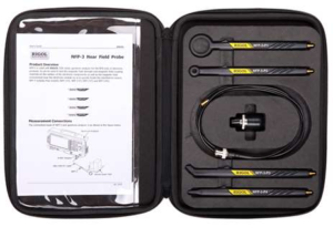
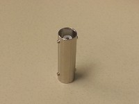
Near Field Probes for Radiated Emissions
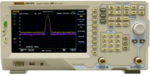
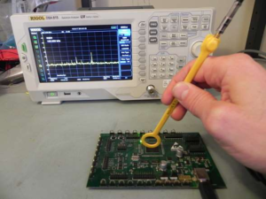
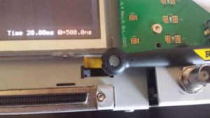
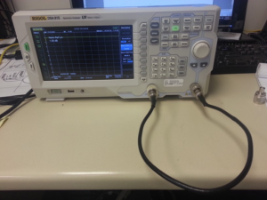
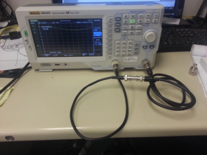
The simplest pre-compliance measurements involve visualizing and analysing the magnetic fields resulting from emissions. These test setups start with a spectrum analyser, like the RIGOL RSA3030 (Figure 1). For radiated emissions, use near field magnetic (H field) probes as shown in Figure 2.
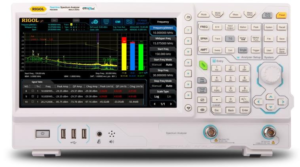
Figure 1: Rigol RSA3000 Spectrum Analyser with EMI
Figure 2: Near Field E and H Probes used to identify EMI Sources
Near field probes pick up emissions that pass through the small loop at the end of the probe. These magnetic probes are relatively inexpensive and make it possible to capture signals only in close proximity to the probe, hence the name ‘near field’ probe. This makes them well suited to basic visualization because engineers can quickly scan a new board or enclosure looking for problems by passing the probe over the area as demonstrated in Figure 3. A basic configuration of a near field radiated emissions test would be simply configuring the analyser to use the peak detector and set the RBW and Span for the area of interest per the regulatory requirements for your device. The Peak detector will provide you with a “worst case” reading on the radiated RF and it is the quickest path to determining the problem areas. Then select the proper H field probe for your design and scan over the surface of the design. Larger probes will give you a faster scanning rate, albeit with less spatial resolution.
The probes act as an antenna, picking up radiated emissions from seams, openings, traces, and other elements that could be emitting RF. A thorough scan of all of the circuit elements, connectors, knobs, openings in the case, and seams is crucial. Chambers and shielding are usually not needed for this type of EMI visualization since the probe registers only very close signals. Engineers can often determine the source of an emission by orienting and locating the probe along the test device. The downside to this approach is that there is no easy correlation between near field measurements and compliance results and making repeatable measurements is difficult due to probe positioning. Therefore, engineers must think critically about detected emissions and determine whether they are worth worrying about before going to the expense of further validation.
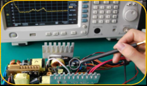
Figure 3: Using an H field probe to test a power supply
RF Current Probes for Conducted Emissions
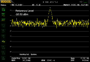
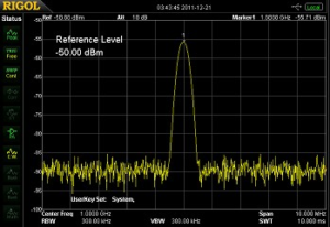
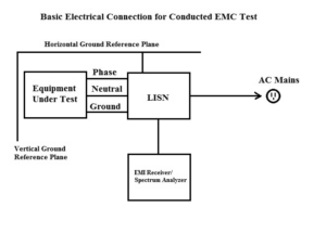
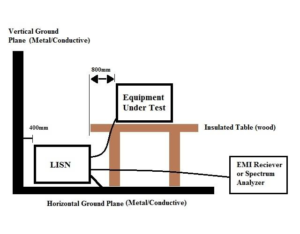
Conducted emissions are unwanted signals that travel via cables. The most common issue is when devices send RF signals back into the power line. There are specific limits associated with these types of emissions designed to protect the power grid and other devices on the circuit. When visualizing conducted emissions engineers use an RF current probe like those in Figure 4. Current flow in a cable placed within the probe is shown on the spectrum analyser. This makes it possible to visualize signals being coupled into a communication or power cable from either the device under test or from external sources. The conducted emissions from a simple LED light fixture are shown in Figure 5. Even simple electronics like this can couple significant power switching frequencies back into the power line. After visualizing these signals care can be taken to filter or improve them if needed before further analysis.
When combined with a spectrum analyser both near field probes and RF current probes are low cost basic visualization solutions for EMI signals. They provide insight without the cost of a more complete EMI system.
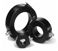
Figure 4: RF Current Probes for Conducted Emissions
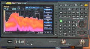
Figure 5: Conducted Emission profile of an LED light fixture
Pre-Compliance Validation Testing
Limits, Standards, Detectors, and Data Management
Once the testing turns to validation, near field measurements still provide important insights, but the wand style probes can be frustrating since slight changes in position or orientation will affect the results. This makes it impossible to compare to standardized test results or even gauge improvement from one version to another. A full compliance setup with calibrated antennas, an EMI receiver, and a chamber could make final compliance tests, but the cost to setup and maintain this setup can be overwhelming. Fortunately, there are tools that help bridge this gap by making relative analysis simpler. With the right setup engineers can evaluate new designs versus known good designs and compare versus established standards. Getting the most out of this type of pre-compliance validation testing requires additional instrumentation capabilities as well as a more stable test setup.
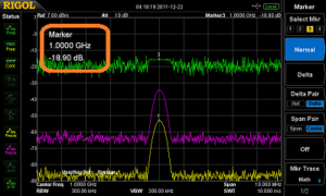
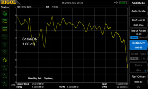
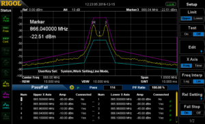
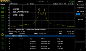
For this type of pre-compliance testing spectrum analysers should include the standard EMI bandwidths and CISPR detectors. The analyser also needs to be able to segment scans using preferred settings for different areas of the spectrum to optimize sweep time and required accuracy. Most importantly, a spectrum analyser must include standard limit lines as well as the ability to customize limit and margin levels. This is critical because without a calibrated chamber alterations must be made for the test environment in order to build confidence in the results. Lastly, the analyser must be able to create, archive, and compare tests and reports so engineers can problem solve any issues or concerns that arise later in the design process. While not an EMI Receiver, RIGOL’s RSA3000 and RSA5000 series spectrum analysers with the EMI application mode (Figure 6) include all of these features in a single box validation solution.
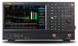
Figure 6: Rigol RSA5000 Series Real-Time Spectrum Analyser with EMI
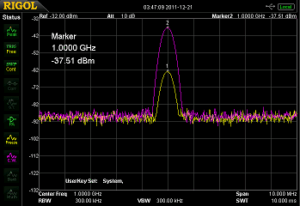
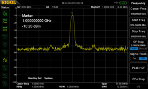
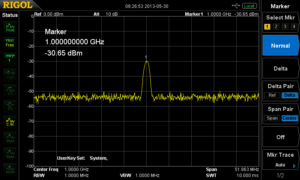
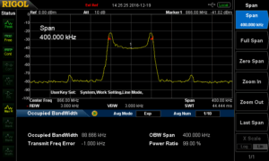
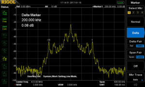
The EMI measurement mode provides the RSA Series spectrum analysers with limits and CISPR detector modes including Quasi-Peak, CISPR Average, and RMS Average. Engineers also have access to the standard EMI resolution bandwidths (200 Hz, 9 kHz, 120 kHz, and 1 MHz). EMI mode (Figure 7) operates entirely within the instrument from the touch screen or with a mouse and keyboard. This makes it easy to archive reports, run scans, and jump to a signal of interest and immediately debug when needed. The bar graph on the right shows real-time measurements at a given frequency of interest. This utility is made to quickly move to a signal of interest right after a scan without having to change modes. It can show live measurements on up to 3 detectors at the frequency of interest providing an easy transition to debugging and further analysis.
For engineers using a common EMI test software platform, their software toolkits provide flexibility by integrating components from multiple test vendors. Many of these pre- compliance software packages support spectrum analysers including models made by RIGOL. All RIGOL spectrum analysers can be programmed over USB or Ethernet using a standard SCPI instruction set.
EMI Mode on the RSA family of spectrum analysers is a powerful solution providing all the capabilities of a complete EMI validation software package within the instrument.
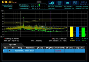
Figure 7: EMI mode using limits, multiple detectors, and meters on a RSA series, Real-Time Spectrum Analyser
TEM Cell setups for repeatable measurements
For a test setup with more repeatable measurements than near field probes we can look to TEM Cells. A TEM (Transverse Electro-Magnetic) Cell (Figure 8) is a low cost alternative to measurements in an anechoic chamber. A TEM Cell is a near field device for radiated and immunity measurements. Because the device under test sits at a fixed location within the cell test results are easier to compare and repeat over time than with just a probe. While not directly correlated to far field chamber measurements, a TEM Cell takes repeatable measurements. When used with a complete EMI application tool, new designs can be compared to known good devices and custom limits can be established or developed from known standards that incorporate background emissions, limitations of the test setup, and correction tables. Used in this way, a TEM cell setup with RIGOL’s EMI Mode builds confidence in final compliance results by making it easy to compare good devices, failed devices, and new designs against corrected limit lines with appropriate margin. A repeatable test setup and RIGOL’s EMI Application mode provide an affordable test bed for EMI pre-compliance validation and comparison.
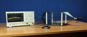
Figure 8: A TEM Cell for repeatable radiated emissions testing
EMI Debugging
Real-Time
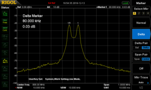
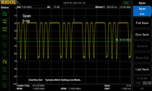
Once validation tests are completed on a new design, areas of concern are identified and require additional debugging or trouble shooting. Emission issues not captured by basic visualization are often dynamic or dependent on the operating state of the design being tested. These issues can be difficult to capture and understand in a typical swept EMI mode. The combination of a repeatable test setup and a real-time spectrum analyser provide additional debugging capabilities. The RIGOL RSA Series analysers provide multiple views valuable in debugging signals that change over time including density, spectrogram, and power vs time (shown in Figure 9 and Figure 10). In real-time mode the RSA is capable of making seamless measurements. Capture a spectrum without sweeping or missing critical signal activity. Debugging in real-time means that infrequency emissions that might affect compliance are easy to characterize, and with a sense of time, it is much easier to establish the ultimate cause in the design.
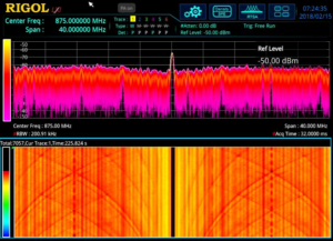
Figure 9: Debugging emissions with the density display (top) and the spectrogram waterfall chart (bottom)
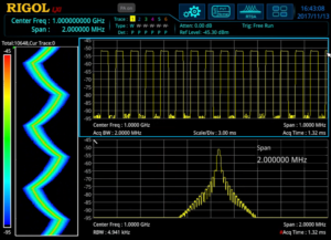
Figure 10: Debugging with a combined view of the spectrum (bottom), power over time (top), and spectogram (left)
Debugging with Time Correlation
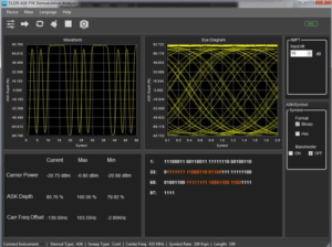
Additionally, the RSAs have an IF Output. For advanced time correlation of emissions events with embedded signals this IF Output can be input into a mixed signal oscilloscope like the RIGOL MSO7054. This brings the RF signal down to a carrier visible to the scope. In this configuration the RF signal can be viewed alongside digital channels to debug embedded code and communications. To learn more about debugging with the IF output go to our Multi Domain Debugging web page.
Testing emissions with real-time debugging and time correlation for root cause analysis in a repeatable TEM Cell setup is a cost effective system configuration for many of the common EMI design challenges.
Unprecedented Value
EMC Compliance testing is mandatory for the majority of electronic products that are slated for sale throughout the world. Select your instruments and design your test setup to get the most out of your EMI budget for any Pre-Compliance use case. With the right spectrum analyser, visualize emissions with near field and RF probes. Then, validate EMI pre-compliance measurements against known emissions data. Finally, debug and time correlate signals of interest to improve the design. These pre-compliance test setups will help speed product development and save time and money in your design process.
Products Mentioned In This Article:
- MSO7054 please see HERE
- RSA3000 Series please see HERE
- RSA5000 Series please see HERE
- TEM Cells please see HERE