EMC Pre-Compliance Testing: Near Field Probing
Solution: Electronic products can emit unwanted electromagnetic radiation, or electromagnetic interference (EMI). Regulatory agencies, such as the FCC in North America, create standards that define the allowable limits of EMI over specific frequency ranges.
Testing designs and products for compliance to these standards can be difficult and expensive. But, there are tools and techniques that can help to minimize the cost of testing and help to enable designs to pass compliance testing quickly.
One of the most often used techniques for EMI testing is near field probing. In this technique, a spectrum analyser is used to measure electromagnetic radiation from a device-under-test using magnetic (H) field and electric (E) field probes.
In this application note, we are going to describe some common techniques used to identify problem areas using near field probes.
A Word about Pre-Compliance
Most governments have regulations in place that specify the amount of electromagnetic interference (EMI) a product can emit into the environment (radiated emissions) and conduct down the power cord (conducted emissions).
Products being sold within the areas covered by these regulations must comply with the defined test limits. Compliance tests use these regulations to define the proper instrumentation, physical setup, and experimental techniques and experience to correctly record and report properly. This testing is very important and required for legal sale of the product within the covered area. Unfortunately, compliance testing can be expensive and difficult to execute due to the specialised equipment and knowledge required to properly conduct the tests.
Pre-compliance testing simulates the major details of a compliant test setup at a lower investment in time and money. Before you go to a compliance lab for testing, you can use pre-compliance tests to gather information about the performance of a design, make changes (if needed), and retest.. all in an effort to minimize the return trips to the compliance lab.
A word of caution, however. Pre-compliance data can be useful in hunting down many, if not all, of the non-compliant areas of a design but it is not a substitute for testing at a fully accredited compliance lab. Ultimately, the company (you) is responsible for proof of compliance to the full regulations for your product.
Setup
Board level emission testing can be performed using a spectrum analyser, like the Rigol DSA-815 (9kHz to 1.5GHz), near field electric (E) and magnetic (H) probes, and the appropriate connecting cable.
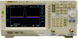
Figure 1: The Rigol DSA815-TG Spectrum Analyser.
A commercial example of near field probes are the Rigol NFP-3 probes shown below:
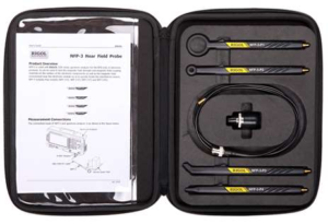
Figure 2: Rigol NFP -3 EMC probes.
You can also build your own probes by removing a few cm of outer shield and insulator from a semi-rigid RF cable, bending it into a loop, and dipping in plastic tool dip or other insulating material. Larger diameter loops will pick up smaller signals, but do not have as much spatial resolution as smaller diameter loops.
For the first pass, configure the spectrum analyser to use the peak detector. This setting ensures that the instrument is capturing the “worst case” peak RF. It also provides a fast scan rate to minimize the time spent at one position as you scan over your DUT. Larger probes will give you a faster scanning rate, albeit with less spatial resolution. Smaller probes, like the E Field probe, provide fine spatial resolution and can be used to detect RF on single pins of circuit elements.
Probe orientation (rotation, distance) is also important to consider. The probes act as an antenna, picking up radiated emissions. Exposing the loop to the largest perpendicular field possible will maximize the signal strength. You can also use a fixture to hold both the Device-Under-Test (DUT) and the probe. This will help create repeatable measurements and minimize differences in measurements due to probe orientation.
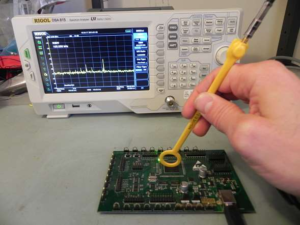
Figure 3: An example of using an H field probe and spectrum analyser to find trouble spots on a board. Note the orientation of the H field probe
Take care to test enclosure seams, openings, traces, and other elements that could be emitting RF. A thorough scan of all of the circuit elements, connectors, knobs, openings in the case, and seams is crucial to identifying potential areas where RF can “leak” out of an enclosure.
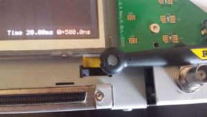
Figure 4: Measuring a display ribbon cable for emissions using an H field probe.
You can use tinfoil or conductive tape to cover suspected problem areas like vents, covers, doors, seams, and cables coming through an enclosure. Simply test the area without the foil or tape, then cover the suspected area, and rescan with the probe.
Once you have identified the physical locations of the areas that have the highest emissions, you can get more detail by implementing a few common techniques. If possible, select a spectrum analyser that has the standard configuration used in full compliance testing. This includes a Quasi-Peak detector mode, EMI filter, and Resolution Bandwidth (RBW) settings that match the full test requirements specified for your product.
This type of setup will increase testing time but should be used on the problem areas. A full compliance test utilizes these settings.. and so, your pre-compliance testing with this configuration will provide a greater degree of visibility into the EMI profile of your design.
Conclusion
In closing, near field probes and a spectrum analyser can be useful tools in troubleshooting EMI issues.
– With H field probes, try different probe orientations to help isolate problem
areas
– Remember to probe all of the seams around any enclosure surrounding electronic components/boards.. surface contact and finish effect grounding and shielding
– Openings in enclosures radiate just like solid structures. They act like
antennas.
– Ribbon cables and cables/inputs with bad shielding and grounds are common causes of radiated emissions
Products Mentioned In This Article:


